


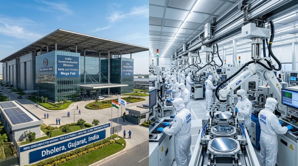
India’s ambition to emerge as a premier global hub for chip manufacturing has gained historic momentum under the India Semiconductor Mission 2026. Tata Electronics, in technical partnership with Taiwan’s Powerchip Semiconductor Manufacturing Corporation (PSMC), has accelerated civil and cleanroom construction at its flagship ₹91,000-crore commercial semiconductor fabrication plant located in the Dholera Special Investment Region (SIR). The milestone marks the physical foundation of the nation’s high-tech manufacturing sovereignty.
Fast-Tracking the Dholera Mega Fab Infrastructure
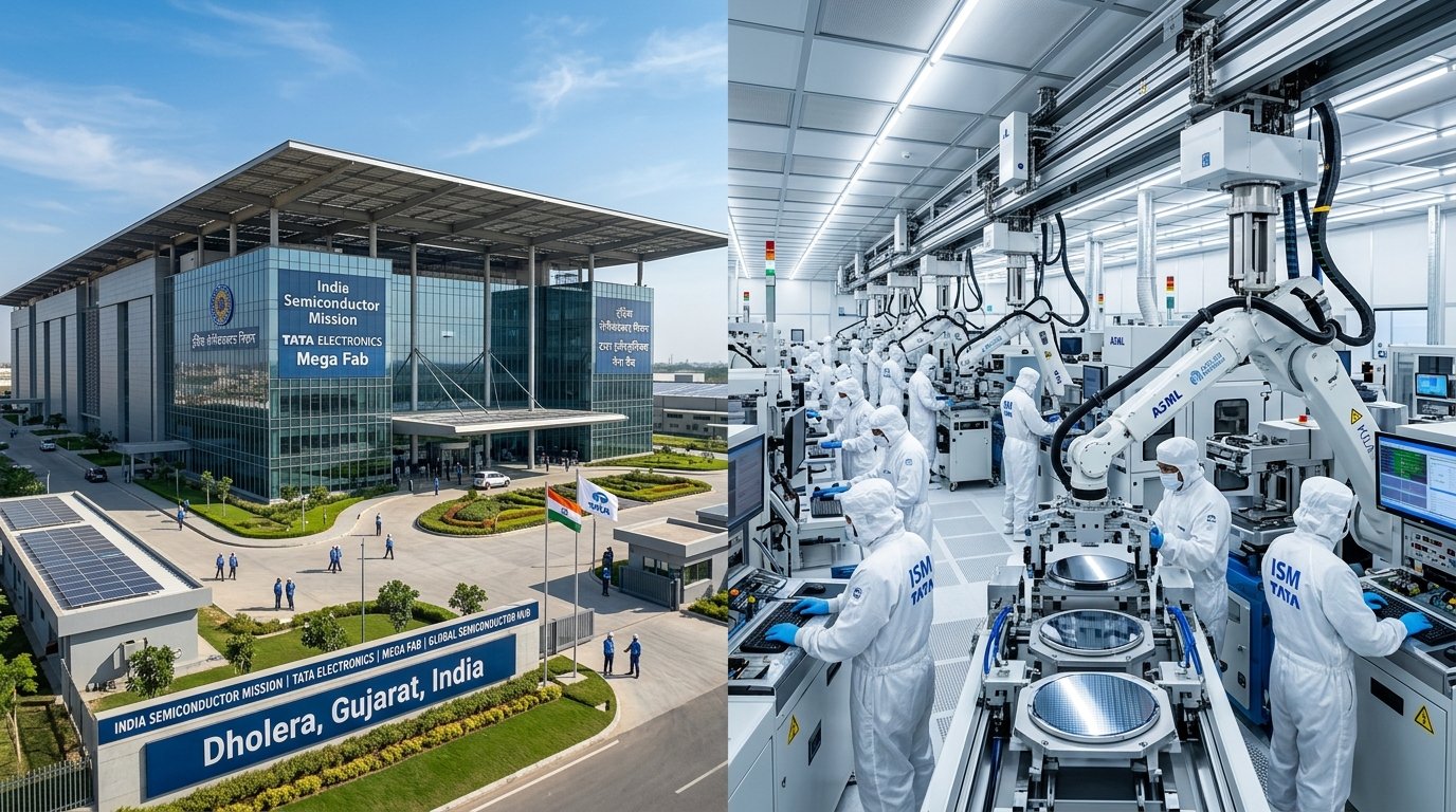
The Dholera facility represents India’s first commercial wafer fabrication plant, designed to produce up to 50,000 silicon wafers per month at full capacity. Guided by the strategic policy imperatives of the India Semiconductor Mission 2026, the plant focuses on mature and specialized technology nodes, including 28-nanometer, 50-nanometer, and 90-nanometer fabrication processes.
These specialized semiconductor nodes serve as the workhorse silicon chips required by global automotive manufacturers, telecommunications network providers, power electronics suppliers, and defense electronics systems. Consequently, establishing indigenous fabrication eliminates critical import vulnerabilities while embedding Indian engineering into the international microelectronics supply chain.

Launch of the 363-Acre Semiconductor Vendor Park
To support round-the-clock commercial operations, the government and Tata Electronics have simultaneously designated a 363-acre dedicated semiconductor ecosystem and vendor park directly adjacent to the main fab complex. This specialized zone will house global and domestic suppliers specializing in:
- Ultra-Pure Industrial Chemicals and Gases: Dedicated facilities for electronic-grade bulk gases, hydrogen, nitrogen, and precision chemical reagents.
- Precision Quartzware and Silicon Slicing: In-situ component machining to support continuous cleanroom operations without international supply interruptions.
- Advanced Assembly and Testing (OSAT): Complementary packaging operations to streamline the journey from raw silicon ingot to final tested microchip.
- Clean Energy and Water Recycling: Integrated zero-liquid-discharge water treatment delivering millions of liters of ultra-pure water (UPW) daily.
Synergy with Nationwide Infrastructure and Tech Expansion
The technological leap achieved under the India Semiconductor Mission 2026 harmonizes with broad infrastructure modernizations underway across the country. Just as large-scale civil projects like Rajasthan’s ERCP project Rajasthan 2026 secure essential agrarian water resources and civic initiatives like the Ayad River rejuvenation Udaipur upgrade urban corridors, high-technology megafabs secure national digital infrastructure.
Furthermore, regional connectivity upgrades such as the Udaipur airport expansion provide direct transit links for technical specialists and semiconductor supply-chain executives commuting between Gujarat’s Dholera industrial zone and regional innovation centers across Western India.
Workforce Development and Global Partnerships
According to policy guidelines updated by the Ministry of Electronics and Information Technology (MeitY), specialized talent cultivation programs have been embedded across premier engineering universities to train over 20,000 semiconductor cleanroom operators and design engineers by late 2026. Taiwanese master trainers from PSMC are currently conducting intensive training cohorts for Indian lead engineers.
With civil structures advancing ahead of targeted schedules, pilot production runs remain firmly scheduled for late 2026, fulfilling a multi-decade technological ambition and cementing the India Semiconductor Mission 2026 as an engine of global microchip innovation.