Office Address
14, Residency Road, Udaipur, Rajasthan 313001
Office Address
14, Residency Road, Udaipur, Rajasthan 313001

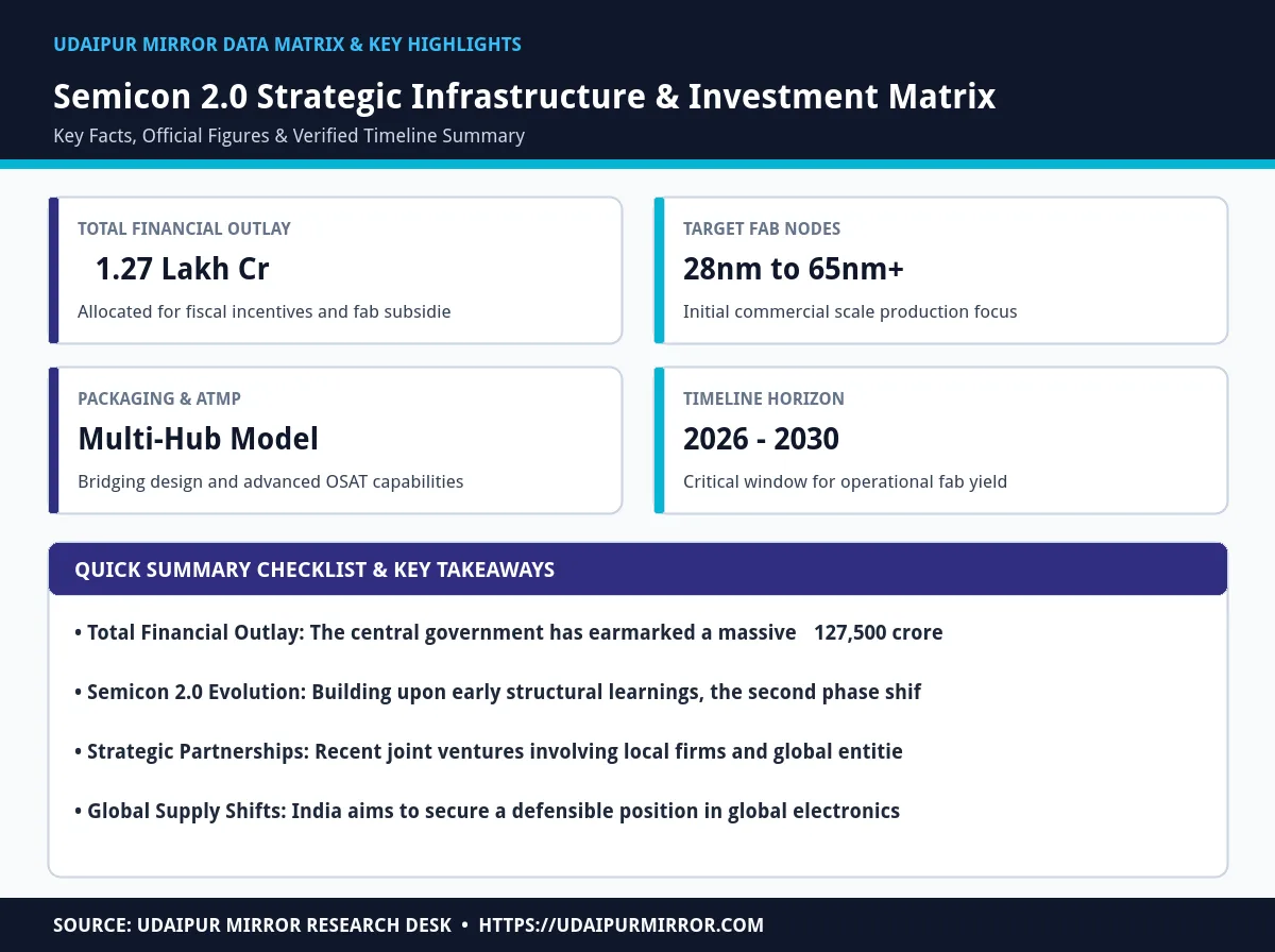
NEW DELHI: NEW DELHI — As global supply chains realign in the wake of geopolitical shifts, India is doubling down on its domestic manufacturing ambitions with an unprecedented semicon 2.0 semiconductor push backed by a massive financial outlay. With a cumulative budgetary commitment touching ₹127,500 crore, policymakers, industry veterans, and tech investors are asking a fundamental question: Can this renewed aggressive framework finally break through decades of historical inertia, regulatory bottlenecks, and missed industrial milestones?
⚡ Quick Highlights: India's ₹1.27 Lakh Crore Semiconductor Push: Semicon 2.0 Analyzed
India’s quest for domestic semiconductor manufacturing is not a new narrative. Proposals dating back to the 1980s and early 2000s repeatedly stalled due to prohibitive capital expenditures, uncertain power and water supplies, and a lack of downstream electronics consumption. While India successfully established itself as a global software and IT services hub, hardware manufacturing lagged significantly, forcing the country to import nearly all of its silicon requirements.
Furthermore, industrial sectors have experienced fluctuating macroeconomic pressures; for instance, while industrial equipment manufacturers and renewable energy firms like those tracked in our analysis of Siemens Q2 FY27 Results and Annu Projects Solar Win Lead Buzzing Stocks Today show robust growth, heavy technology hardware manufacturing requires long-term capital stability that previous policy iterations failed to guarantee.
“Building a semiconductor ecosystem is less about writing checks and more about nurturing a symbiotic web of chemical suppliers, ultra-pure water systems, and relentless engineering talent.” — Senior Industrial Technology Analyst
To understand the paradigm shift in India’s technology roadmap, market analysts often compare the initial policy incentives with the expanded framework of Semicon 2.0. The table below outlines the core differences in scope, target areas, and execution strategies.
| Policy Parameter | Phase 1 (Initial Framework) | Semicon 2.0 (Current Evolution) | Strategic Impact |
|---|---|---|---|
| Primary Focus | Basic silicon fabrication & display fabs | Advanced packaging, ATMP, compound semis, ECMS | Broader value chain capture |
| Incentive Structure | Up to 50% capital support for large fabs | Enhanced fiscal backing + design-linked incentives | Lower entry barrier for startups |
| Ecosystem Integration | Siloed manufacturing plants | Collaborative clusters with global packaging firms | Faster time-to-market and testing |
| Talent Development | Basic academic curriculum updates | Specialized 6-month AI and hardware security modules | Targeted industry-ready workforce |
| Raw Material Support | Limited domestic chemical sourcing | Dedicated Electronic Component & Material Subsidies | Reduced import dependency |
The newly minted Semicon 2.0 framework addresses historical shortcomings by expanding beyond basic silicon wafer fabrication. Recognizing that the global chip shortage and geopolitical tensions have made supply chain resilience paramount, the government has broadened subsidies to cover compound semiconductors, Advanced Packaging, Test, Marking, and Packaging (ATMP) units, and Electronic Component and Material Sourcing (ECMS).
By lowering the entry barriers for specialized design startups and supporting strategic joint ventures—such as recent tie-ups between domestic firms like Paras Semiconductors and global packaging specialists like BroadPak—India is creating localized pockets of expertise. Meanwhile, software development agencies and tech firms looking to scale operations can leverage insights from guides like the 10 Best Mobile App Development Companies in India (2027 Edition): Top Agencies, Cost & Tech Guide to understand the broader digital transformation wave sweeping across Indian metropolitan hubs.
“Semicon 2.0 acknowledges that you don't necessarily need to capture the absolute bleeding-edge 2nm node immediately to win; mastering advanced packaging and specialty nodes is the pragmatic gateway.” — Venture Capital Partner, DeepTech Fund
As India rolls out its ₹127,500 crore initiative, the global semiconductor landscape faces unprecedented turbulence. International supply chains remain vulnerable to trade restrictions, talent shortages, and corporate scandals involving major industry leaders. Navigating these turbulent waters requires strategic diplomacy, highlighted by recent bilateral initiatives like the India-France Critical Technologies Dialogue, which seek to secure resilient tech corridors.
Domestically, macroeconomic factors such as currency fluctuations and import duties also play a role in how retail and industrial tech hardware is priced. While global bullion adjustments—similar to trends noted in reports covering how Gold Falls 21.4% Globally From Peak, But Rupee Depreciation and Higher Import Duties Limit India’s Retail Impact—affect broader import dynamics, electronic hardware procurement must maintain insulation from sudden forex shocks through robust domestic substitution.
“Geopolitical realignment is our generational window. If India fails to anchor its semiconductor supply chain now, domestic industries will remain permanently vulnerable to external shocks.” — Policy Strategist, New Delhi
Transforming India into a global semiconductor hub ultimately hinges on human capital. Designing, fabricating, and testing microchips requires specialized engineering disciplines that traditional university syllabi have historically underserved. To bridge this divide, academic institutions and industry bodies are launching targeted micro-credentials, such as specialized cybersecurity and hardware security programs designed to prepare engineers for clean-room and fabless chip design environments.
Looking forward to 2030, the success of the semicon 2.0 semiconductor push will be measured not by the number of Memorandums of Understanding signed, but by functional commercial wafer output, sustainable water and power management, and the integration of Indian-designed silicon into global consumer electronics, automotive systems, and AI infrastructure.
“Our universities are finally aligning with industrial realities. The next batch of engineers won't just write code; they will tape out silicon.” — Academic Lead, VLSI Design Center
The central government has committed a massive financial corpus of ₹127,500 crore to incentivize semiconductor fabrication, advanced packaging, and raw material ecosystems.
While Phase 1 focused heavily on basic silicon wafer fabs, Semicon 2.0 expands support to include advanced packaging (ATMP), compound semiconductors, design-linked incentives, and raw material component sourcing.
Past initiatives often stalled due to prohibitive upfront capital expenditures, unreliable ultra-pure water and power grids, a lack of local downstream electronics consumption, and heavy dependence on foreign supply chains.
Strategic collaborations with global firms (such as BroadPak) and bilateral frameworks (like the India-France Critical Technologies Dialogue) help bridge critical skill gaps, secure intellectual property, and integrate Indian manufacturing into global supply chains.
Add Udaipur Mirror as a preferred source on Google to see more of our travel guides in your AI overviews.