Office Address
14, Residency Road, Udaipur, Rajasthan 313001
Office Address
14, Residency Road, Udaipur, Rajasthan 313001

NEW DELHI: NEW DELHI — Marking a monumental leap forward in India’s ambitious drive toward self-reliance in high-tech hardware, the Union Government has officially rolled out the advanced digital ecosystem. As part of this comprehensive national technology push, india launches semicon 2.0 portal to streamline approvals, fast-track investments, and position the country as a trusted global hub for semiconductor fabrication, OSAT facilities, and electronic component manufacturing.
⚡ Quick Highlights: India Launches Semicon 2.0 Portal with ₹7,503 Cr Approvals
The rollout of the upgraded digital gateway represents a major watershed moment for India’s electronics ministry. Over the past few years, international analysts often questioned the viability of establishing complex semiconductor fabrication plants on the subcontinent given high capital intensity and water-power dependencies. However, aggressive policy incentives, combined with transparent subsidy disbursements, have successfully flipped the narrative.
Union Minister Ashwini Vaishnaw emphasized that the journey from initial skepticism to absolute industrial confidence has been rapid. Global original equipment manufacturers (OEMs) and domestic conglomerates are now betting heavily on the country’s technological future. Concurrently, broader consumer market indicators—such as those observed during Diwali gold buying trends—reflect resilient domestic liquidity that is increasingly finding its way into high-growth manufacturing sectors.
“We have successfully bridged the gap between policy formulation and ground execution. The world now looks at India not as a mere consumer market, but as a core pillar of resilient global semiconductor supply chains.” — Ashwini Vaishnaw, Union Minister for Electronics and IT
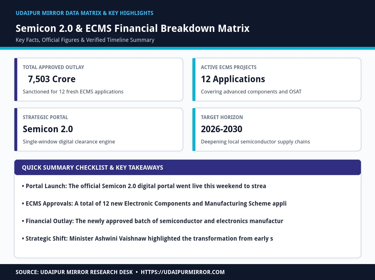
The table below outlines the core pillars, financial metrics, and operational focus areas of the newly introduced Semicon 2.0 framework and its corresponding electronic component manufacturing approvals.
| Initiative Element | Financial Allocation | Target Objective | Implementation Status |
|---|---|---|---|
| Semicon 2.0 Portal | Digital Infrastructure | Single-window clearance & fast-tracking | Active / Live Nationwide |
| ECMS Batch Approvals | ₹7,503 Crore | Funding 12 new component manufacturing units | Approved & Cleared |
| Upstream Supply Chain | Private-Public Synergy | Local fabrication, silicon packaging, & OSAT | Rolling Out Phase-2 |
| Retail & Consumer Impact | Market Broadening | Enhancing domestic electronics hardware output | Ongoing Execution |
At the heart of the latest announcement is the formal approval of 12 fresh applications under the Electronic Components and Manufacturing Scheme (ECMS). These projects collectively command an investment outlay of ₹7,503 crore, targeting critical gaps in the domestic electronics value chain. From passive components and specialized printed circuit boards (PCBs) to advanced testing and packaging equipment, the approved entities span diverse technological sub-sectors.
Industry experts note that while capital markets experience volatility across various global geographies, India’s targeted fiscal incentives provide a safe harbor for technology investors. The localized production of electronic components drastically reduces supply chain vulnerability to external geopolitical shocks.
“Securing robust backing for component manufacturing ensures that downstream industries—from smartphones to automotive electronics—have uninterrupted access to critical hardware.” — Senior MeitY Official
Beyond physical fabrication and component assembly, the Semicon 2.0 initiative integrates robust compute infrastructure to support domestic fabless chip design startups. Semiconductor design requires immense computational power, specialized Electronic Design Automation (EDA) software licenses, and secure cloud storage. The new portal links academic institutions, research labs, and private startups into a unified collaborative grid.
This holistic approach ensures that Indian engineers can conceptualize, simulate, and tape-out advanced system-on-chips (SoCs) locally before sending them to operational fabrication foundries. The integration of high-performance computing clusters is expected to spawn dozens of domestic fabless semiconductor unicorns over the next half-decade. (Also read: Diwali gold buying: Drop in yellow metal prices boosts jewellery sales – Should you buy?).
“Design is where intellectual property is created. By empowering Indian startups with design tools and cloud capacity, we are securing our long-term technological sovereignty.” — Technology Sector Analyst
The launch of Semicon 2.0 occurs against a backdrop of wider global financial turbulence, characterized by multi-trillion-dollar valuations adjustments in Western technology markets and cautious investor sentiment. While international venture capital has tightened purse strings for software-only applications, hard-tech and semiconductor infrastructure continue to attract strategic sovereign capital.
By channeling domestic savings and foreign direct investments into foundational hardware assets, India is effectively insulating its digital economy from external liquidity crunches. This structural shift ensures sustainable, long-term economic momentum independent of short-term global tech corrections.
“Hard-tech investments require patience and strategic foresight. India's commitment to building silicon capabilities provides a stable anchor amid global market shifts.” — Venture Capital Partner
The Semicon 2.0 portal is a newly launched single-window digital platform designed by the Ministry of Electronics and Information Technology (MeitY) to streamline, evaluate, and fast-track semiconductor and electronic component manufacturing applications in India.
The government has approved 12 new Electronic Components and Manufacturing Scheme (ECMS) applications with a total financial outlay of ₹7,503 crore.
The portal and the corresponding ECMS approvals were officially launched and announced by Union Minister for Electronics and IT, Ashwini Vaishnaw.
The core goals include establishing domestic fabrication and OSAT facilities, reducing import dependence for electronic components, fostering fabless chip design startups, and building a self-reliant high-tech manufacturing ecosystem.
Add Udaipur Mirror as a preferred source on Google to see more of our travel guides in your AI overviews.